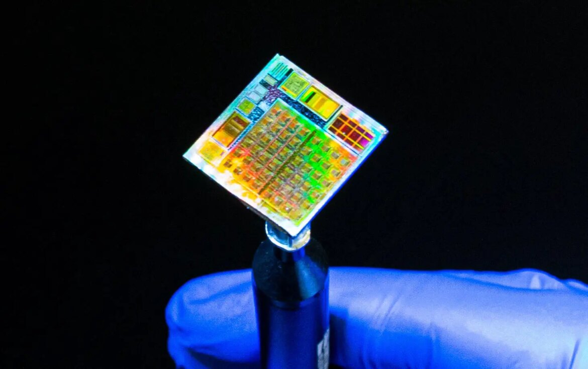
Researchers at KAUST, led by Professor Mario Lanza, have achieved a groundbreaking milestone by successfully developing the world’s inaugural 2D microchip utilizing synthetic materials. Overcoming significant fabrication hurdles, the team has managed to create a chip that operates as a high-performance, low-power neural network component, opening up new avenues for the advancement of microchip technology.
This pioneering demonstration of a functional microchip, seamlessly integrating atomically thin two-dimensional materials with extraordinary properties, marks the dawn of a new era in microelectronics.
The fabrication of the world’s first fully integrated and operational microchip, constructed from exotic two-dimensional materials, has been accomplished at KAUST. This breakthrough showcases the immense potential of 2D materials in augmenting the functionality and performance of microchip-based technologies.
Since the discovery of graphene, which comprises atomically thin layers of graphite, in 2004, there has been immense interest in these materials due to their extraordinary and promising physical properties. However, the practical realization of functional microdevices based on these delicate 2D materials has remained elusive, owing to the challenges associated with their delicate handling and fabrication.
Inspired by recent advancements in Professor Lanza’s laboratory involving functional 2D films, the collaboration led by KAUST has successfully produced and showcased a prototype microchip built on a foundation of 2D materials.
“Our objective was to enhance the technology readiness level of electronic devices and circuits based on 2D materials by utilizing conventional silicon-based CMOS microcircuits as a foundation and employing standard semiconductor fabrication techniques,” explains Lanza. “Nevertheless, synthetic 2D materials often possess local defects, such as atomic impurities, which can lead to the failure of small-scale devices. Furthermore, integrating the 2D material into the microchip without causing damage presented a significant challenge.”
To address these obstacles, the research team optimized the chip’s design, simplifying the fabrication process and minimizing the impact of defects. This involved fabricating standard complementary metal oxide semiconductor (CMOS) transistors on one side of the chip and creating interconnects that extended to the underside. In this manner, the 2D material could be reliably transferred onto small pads measuring less than 0.25 micrometers.
“We synthesized the 2D material, hexagonal boron nitride (h-BN), on copper foil and subsequently transferred it onto the microchip using a low-temperature wet process. We then formed electrodes on top using conventional vacuum evaporation and photolithography, techniques that are readily available to us,” explains Lanza. “By adopting this approach, we constructed a 5×5 array of one-transistor/one-memristor cells interconnected in a crossbar matrix.”
The exceptional properties of the 2D h-BN material, a mere 18 atoms thick or 6 nanometers, render it an ideal “memristor” — a resistive component whose resistance can be controlled by the applied voltage. In this configuration, each microscale memristor pad within the 5×5 arrangement is linked to a dedicated transistor, enabling precise voltage control necessary for the memristor to function as a high-performance device with exceptional reliability over numerous cycles. In this specific case, it serves as a low-power neural network element.
“With this groundbreaking achievement, we are currently engaging in discussions with leading semiconductor companies to further pursue this direction,” asserts Lanza. “Moreover, we are contemplating the installation of our own wafer-scale industrial processing system for 2D materials at KAUST to advance this capability.”
Reference: “Hybrid 2D–CMOS microchips for memristive applications” by Kaichen Zhu, Sebastian Pazos, Fernando Aguirre, Yaqing Shen, Yue Yuan, Wenwen Zheng, Osamah Alharbi, Marco A. Villena, Bin Fang, Xinyi Li, Alessandro Milozzi, Matteo Farronato, Miguel Muñoz-Rojo, Tao Wang, Ren Li, Hossein Fariborzi, Juan B. Roldan, Guenther Benstetter, Xixiang Zhang, Husam N. Alshareef, Tibor Grasser, Huaqiang Wu, Daniele Ielmini and Mario Lanza, 27 March 2023, Nature.
DOI: 10.1038/s41586-023-05973-1
Table of Contents
Frequently Asked Questions (FAQs) about 2D microchip technology
What is a 2D microchip?
A 2D microchip refers to a microchip that incorporates atomically thin two-dimensional materials, such as graphene or hexagonal boron nitride (h-BN), into its design. These materials possess unique properties that can enhance the functionality and performance of microchip-based technologies.
How significant is the development of a functional 2D microchip?
The development of a functional 2D microchip is highly significant. It represents a major breakthrough in microelectronics, as it demonstrates the potential of utilizing exotic 2D materials in creating fully integrated and operational microchips. This achievement paves the way for advancements in microchip technology and opens up new possibilities for electronic devices.
What are the challenges in fabricating 2D microchips?
Fabricating 2D microchips presents several challenges. One major hurdle is the delicate nature of the 2D materials, which can be easily damaged during the integration process. Additionally, synthetic 2D materials often contain local defects, such as atomic impurities, that can impact the performance of the microchip. Overcoming these challenges requires optimizing chip designs, employing specialized fabrication techniques, and minimizing the effects of defects.
What is the potential application of 2D microchips?
2D microchips have a wide range of potential applications. Their high-performance and low-power characteristics make them suitable for various electronic devices. In this particular case, the demonstrated 2D microchip functions as a low-power neural network element. Additionally, the integration of 2D materials into microchips can enhance the functionality and performance of diverse microchip-based technologies, such as sensors, processors, and memory devices.
What are the future prospects of 2D microchips?
The successful development of a functional 2D microchip marks an important milestone in the field of microelectronics. This breakthrough has generated significant interest from leading semiconductor companies, and further collaborations are being pursued. The researchers are also considering the installation of a wafer-scale industrial processing system for 2D materials, which would advance the capabilities and scalability of 2D microchip technology.
More about 2D microchip technology
- “Hybrid 2D–CMOS microchips for memristive applications” – Link: DOI: 10.1038/s41586-023-05973-1
- KAUST Website – Link: https://www.kaust.edu.sa


